
Electromagnetic Compatibility (EMC) noise can cause significant issues for electronic devices, from minor glitches to complete operational failure. To ensure reliable performance and regulatory compliance, it is essential to implement effective techniques to reduce EMC noise. This article will explore various methods to minimize electromagnetic interference (EMI) and enhance the EMC performance of your electronic devices.
Understanding EMC Noise
What Is EMC Noise?
EMC noise, also known as electromagnetic interference (EMI), refers to unwanted electrical signals that disrupt the normal functioning of electronic devices. EMI can occur through both conducted and radiated emissions, which interfere with the performance of the device and, in some cases, may even cause safety hazards.
Causes of EMC Noise
EMC noise can be caused by several factors, including both natural and man-made sources. Common sources include:
-
Electrical Equipment: Devices such as mobile phones, computers, industrial machinery, and communication equipment often emit electromagnetic radiation that can interfere with nearby systems.
-
Power Lines: High-voltage power lines can generate electromagnetic fields that disrupt nearby electronics.
-
Poor Grounding and Shielding: Insufficient grounding or shielding in the device design can allow unwanted EMI to pass through the system, leading to operational issues.
-
Environmental Factors: Natural events like lightning or solar flares can also create electromagnetic interference.
Techniques to Reduce EMC Noise
Several techniques can help reduce the impact of EMC noise on your electronic devices. The following methods address the primary sources of interference and can significantly improve device performance.
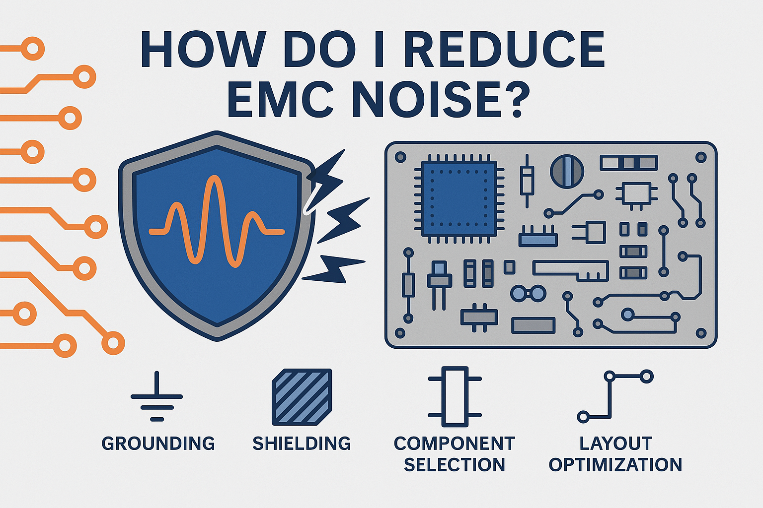
1. Proper Grounding
Grounding is one of the most effective ways to mitigate EMI. By connecting the device to a ground plane or earth ground, you create a low-impedance path for unwanted electrical signals to dissipate. Proper grounding allows excess EMI to flow safely to the ground, preventing it from entering the sensitive components of the device.
-
Low Impedance Path: Ensure that the grounding path has minimal impedance to efficiently redirect the unwanted signals.
-
Dedicated Grounding Systems: Use a dedicated grounding system for sensitive equipment to minimize noise from other electrical devices in the same environment.
2. Shielding
Shielding is another critical method for reducing EMC noise. It involves enclosing the device in a conductive material, such as metal, which reflects or absorbs unwanted electromagnetic radiation. Shielding is especially effective in preventing radiated emissions from escaping or external interference from entering the device.
-
Materials for Shielding: Materials such as aluminum, copper, and stainless steel are commonly used for shielding due to their excellent conductivity.
-
Shielding Enclosures: Enclosing sensitive components in metallic enclosures can prevent external EMI from affecting the device’s operation.
3. Use Low-Noise Components
Selecting components that are designed to minimize electrical noise can significantly reduce the generation of EMI in the first place. Using high-quality components ensures that the device operates with minimal interference.
-
Low-Noise Power Supplies: Opt for low-noise power supplies that minimize the generation of electromagnetic radiation. Switch-mode power supplies (SMPS) can sometimes generate noise, so using linear power supplies or specially designed low-noise SMPS units can help reduce emissions.
-
High-Quality Capacitors: Choose capacitors that are designed to filter out noise and smooth power delivery.
4. Optimized Layout and Routing
Proper PCB (Printed Circuit Board) layout and component placement are crucial in minimizing EMI. Strategic placement of components and signal traces can help reduce the coupling of noise.
-
Component Placement: High-speed components that generate a lot of noise should be placed away from sensitive components to prevent interference.
-
Minimize Parallel Runs: Keep the lengths of parallel signal traces to a minimum, as long parallel runs can act as antennas and increase EMI.
-
Use Ground Planes: Employ dedicated ground planes to isolate noisy components and ensure that noise does not spread across the PCB.
5. Ferrite Beads and Cores
Ferrite beads and cores are passive components that can help suppress high-frequency noise. They are typically placed on power and signal lines to filter out EMI and prevent it from traveling through the circuit.
-
Placement of Ferrites: Use ferrite cores on cables entering or leaving the device, especially near power supplies and input/output (I/O) lines.
-
Ferrite Material Selection: Select appropriate ferrite materials for the specific noise frequency range you want to suppress.
6. Decoupling Capacitors
Decoupling capacitors are used to filter out high-frequency noise and stabilize voltage levels within the circuit. By placing decoupling capacitors close to power supply pins on the PCB, you can reduce the chances of noise affecting sensitive components.
-
Placement: Position the capacitors as close as possible to the power pins to ensure efficient noise suppression.
-
Bypass Capacitors: Use bypass capacitors in parallel with decoupling capacitors to ensure smoother power delivery and minimize noise coupling.
7. Spread Spectrum Clocking
Spread spectrum clocking is a technique where the clock frequency is varied over time. This reduces the peak emissions by spreading the energy over a wider frequency range, which helps in reducing EMI.
-
Clock Frequency Variation: By introducing slight variations in the clock frequency, the energy is distributed over a broader bandwidth, reducing the intensity of noise at any single frequency.
-
Implementation: This method can be implemented in devices that use clock generators or oscillators, particularly in high-speed circuits.
8. Differential Signaling
Differential signaling involves transmitting the same electrical signal in two complementary (positive and negative) forms over two separate wires. This method reduces the electromagnetic field generated by the signal, minimizing EMI.
-
Benefits of Differential Signaling: It reduces the likelihood of noise coupling and improves the immunity of the signal to external interference.
-
Applications: Differential signaling is commonly used in high-speed data transmission systems, such as USB, Ethernet, and serial communication standards.
Managing Ambient EMI
Ambient EM Noise Check
Before starting EMI troubleshooting, it’s essential to assess the ambient electromagnetic noise in your testing environment. Common sources of ambient noise include:
-
Dirty Mains Network: Electrical noise from a polluted power supply can affect conducted emission results.
-
Power Supply Noise: The power supply itself can generate both conducted and radiated noise, especially if it is a switched-mode power supply.
-
Nearby Electronic Devices: Devices like laptops, printers, and other equipment in the vicinity can contribute to ambient noise levels.
Suppressing Ambient Noise
To effectively reduce ambient noise, consider the following methods:
-
Location: If possible, choose a dedicated room for EMC testing, such as a basement or underground room, which may offer some natural shielding from external noise.
-
Power Quality Check: Use an isolated HV probe connected to an oscilloscope to check the quality of the mains network. If necessary, add high-quality filters to reduce noise in the power lines.
-
Ferrite Cores: Add ferrite cores to both input and output cables to suppress noise in lower frequency ranges.
-
Nearby Equipment: Turn off nearby equipment, including lights, to minimize external noise interference during testing.
Reducing EMI for Regulatory Compliance
To comply with regulatory standards such as the FCC Part 15 (USA) and EMC Directive (EU), devices must meet certain limits for EMI emissions and have sufficient immunity to external interference. By implementing the techniques discussed above, including grounding, shielding, and optimizing component placement, you can ensure that your device adheres to these regulations and operates reliably in its electromagnetic environment.
For more information, please refer to our article “What is the meaning of EMC shielding?” to explore the necessary steps for ensuring your device meets EMC standards.

